Application Hub · Grade Selection
Semiconductor & Electronics
From wafer slicing and lapping to CMP polishing and chamber cleaning.
Sub Applications
Solutions In This Category
Semiconductor manufacturing is the most demanding application for diamond micron powder: sub-micron PSD control, low metal contamination and stable slurry behaviour all have to hold at the same time. We supply monocrystalline, polycrystalline and detonation grades for wafer slicing, lapping, CMP and chamber maintenance, with nickel and titanium coatings where bond retention is critical.
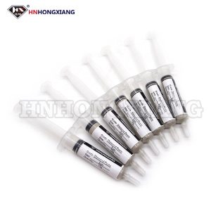
CMP Pad Conditioners And Diamond SlurriesHigh-grade monocrystalline grit for CMP pad conditioners, plus polycrystalline, detonation and nano diamond for CMP slurries.
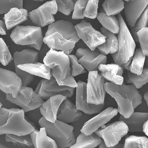
Diamond Powder For Semiconductor Chamber Cleaning ToolsHigh-purity demagnetised diamond powder for CMP chamber scrub pads, cleaning pads and tips.
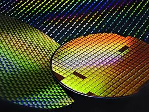
Diamond Wire Sawing of Silicon & SapphireDiamond wire sawing is the dominant method for slicing silicon wafers (photovoltaic and semiconductor) and sapphire ingots. The...
SiC & Sapphire Wafer PolishingSilicon carbide and sapphire substrates demand damage-free, high-precision polishing. Polycrystalline and nano grades deliver low surface roughness with
Diamond Grades For This Category
| Process step | Grade direction | Size range |
|---|---|---|
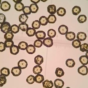
| Wafer slicing (wire saw) | Nickel-coated HDY 56% | 6–12, 8–16, 10–20 µm |
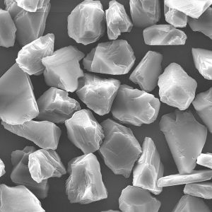
| Wafer lapping & fine polishing | Monocrystalline / polycrystalline micron | 0–1, 1–2, 2–4 µm |
| CMP pad conditioning | Monocrystalline grit, sintered / brazed / electroplated | 80#–270# (50#–325#) |
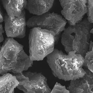
| CMP slurry | Mono-, poly- and detonation nanodiamond | 0.5–60 µm full series |
| Chamber cleaning tools | High-purity demagnetised powder | 80#–400# |
Selection Notes
How To Choose The Right Grade
- Match the grade to the process step, not to the wafer size: slicing needs impact strength, CMP needs a narrow PSD and a low scratch count.
- For CMP slurries ask for the full PSD curve and the metal-ion content — D50 alone does not predict scratch performance.
- Nickel-coated grades lift retention in resin bond and electroplated wire; always specify coating weight as a percentage.
Inquiry
What To Include
Start from the application requirement. We will help narrow the grade, particle size and packing route.
1Wafer or substrate material and diameter
2Process step (slicing / lapping / CMP / cleaning)
3Target removal rate and surface finish (Ra)
4Bond system and coating preference
5Current defect or scratch issue